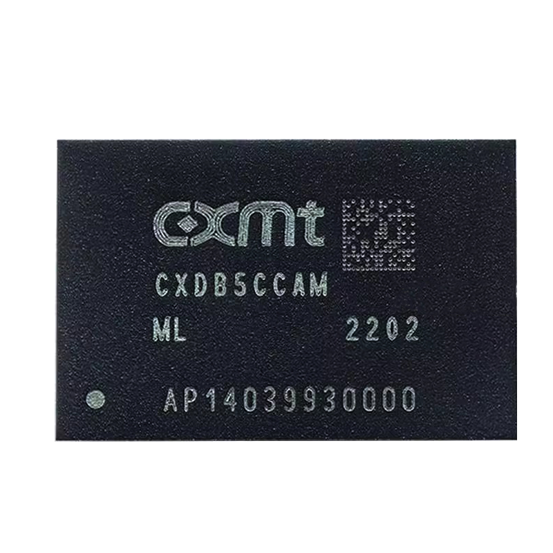
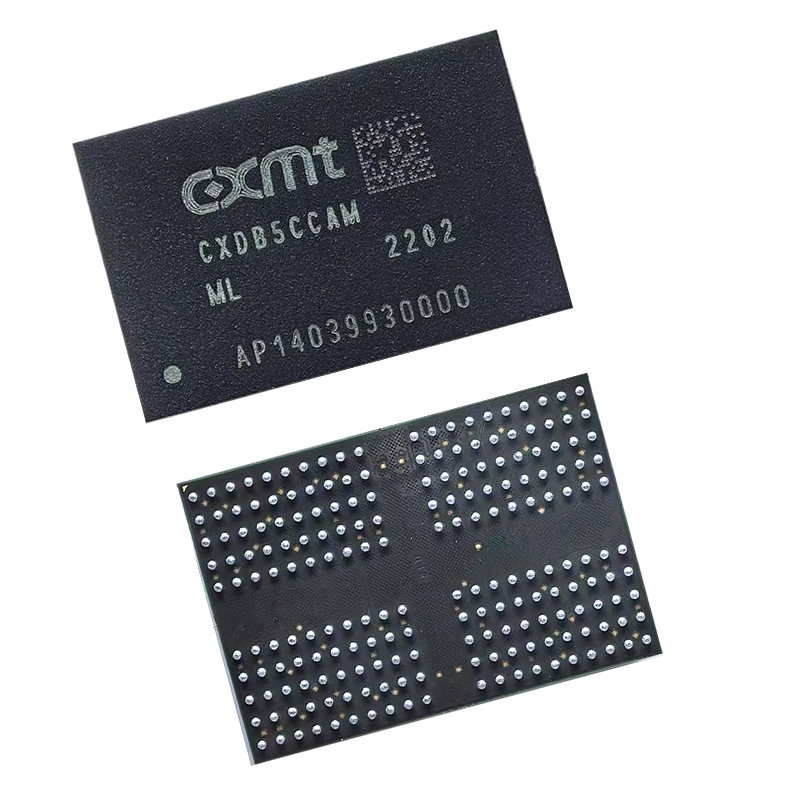
LPDDR4 4GB Computer And Mobile Phone Operating Memory Chip CXDB5CCAM-ML
Clock: CK-T and CK-C are differential clock inputs. All address, command and control input signals are collected when the rising edge of CK-T and the falling edge of CK-c intersect. The AC timing reference of the CA parameter is CK. Each channel (A and B) has its own time.
Clock enable :CKE HIGH activates the internal clock lightning circuit, Hander and Hander, while CKELOW deactivates them. The CKE is part of the command code to switch between entering and exiting energy-saving modes through the bear shape of CKE. Each channel (A and B) has its own CKE signal.
Chip selection :CS is part of the command code. Each channel (A and B) has its own CS signal
Instruction/Address input: The CA signal provides instruction and address input based on the instruction truth table. Each channel (A&B) has its own CA signal.
Data input/output: Bidirectional data bus.
Data selection signals :DQS t and DQSc are bidirectional differential output clock signals used to select the data during read or write operations. During the reading operation, the data selection communication is generated by DRAM and synchronized with the data signal. During the write operation, the data selection signal is generated by the memory controller and must be superior to the arrival of the data signal. Each data byte has a corresponding data selection communication pair. Each channel (A and B) has its own DQS selected communication number.
Data mask inversion :DMI is a bidirectional signal. When the data on the data bus is reversed, DMI is driven to high relevel, or when the normal data is less than the normal state, DMI is passively driven to low level. The data inversion function can be disabled through the mode register Settings. Each data byte has a DMI signal. Each channel (A and B) has its own DMI signal. This signal, along with the DQ signal, provides write data mask information to the DRAM. The function of the DMI pin - data inversion or data mask - depends on the mode register Settings
Packaging and transportation instructions
- According to the standard export packaging.
Customers can choose from cartons, wooden cases and wooden pallets according to their own requirements.
Q&A
1. How to obtain the price?
We usually quote within 24 hours after receiving your inquiry (except weekends and holidays). If you are in urgent need of a price, please send us an email or contact us in any other way so that we can provide you with a quotation.
2. What is your delivery time?
This depends on the quantity of the order and the season in which you place the order. Usually, we can ship the goods within 7 to 15 days (for small batches), and for large batches, it takes about 30 days.
3. What are your payment terms?
Factory price, 30% deposit, 70%T/T payment before shipment.
4. What is the mode of transportation?
It can be transported by sea, air or express delivery (EMS, UPS, DHL, TNT, FEDEX, etc.). Please confirm with us before placing an order.
5. How do you help our business establish a long-term and good relationship?
We maintain good quality and competitive prices to ensure that our customers benefit.
2. We respect every customer as our friend. We do business with them sincerely and make friends with them, no matter where they come from.
Product Tags:

|
|
LPDDR4 4GB Static Ram Chips Computer Mobile Phone Operating Memory CXDB5CCAM-ML Images
|